Microscopy, Electron Scanning
The scanning electron microscope (SEM) enables the imaging of surfaces at very high resolution. The SEM was a development of the earlier transmission electron microscope (TEM), and is a close analog of the conventional optical microscope but uses high- energy electrons instead of photons. This enables it to have a very much higher resolution because, for example, the wavelength of a high-energy (c.100 kilovolt) electron is less than 1/10000 that of a photon of blue light.
The specimen in a TEM has to be very thin so that the electrons can pass through and be focused by electron lenses on to a fluorescent screen to produce the magnified visible image. Surfaces can be imaged directly only with difficulty with a TEM, at a glancing angle. In a SEM, an electron beam probe interacts with the surface producing backscattering and emission of secondary electrons as the high-energy electrons strike the surface; the electron beam is scanned over each part of the surface in turn (pixels), and scattered and secondary electrons for each position in the scan are detected, usually by a cathode ray oscilloscope.
The inventors of the TEM were Max Knoll and Ernst Ruska at the Technische Hochschule, Berlin in the early 1930s, while the development of the SEM started a few years later, also by Knoll after he moved to the Telefunken Company and was working on the development of television iconoscope-type camera tubes. In the course of this work he built an electron beam scanner (1935) for studying the secondary-electron emitting properties of the iconoscope targets.
This apparatus (Figure 2) had many of the features of a modern SEM—the electron beam was scanned to produce a 200-line, 50-fields per second horizontal line scanning (raster), and a cathode-ray tube, deflected in synchronism with scanning of the specimen and modulated in brightness by the secondary electron current from the specimen (labeled ‘‘plate’’ in Figure 2), displayed a visible image. This current depended on the elemental constituents of the specimen surface and, if etched, its topography; but the scanner lacked one essential feature of an SEM, a highly “demagnified” probe.
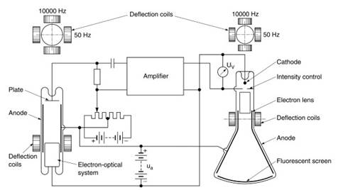
Figure 2. Diagram of Knoll’s 1935 electron beam scanner
In the SEM, magnification is simply the ratio of the different scanned areas at the sample and at the image. Higher magnification comes from scanning a smaller area with a sharply focused beam, made by the SEM electromagnetic lenses. Knoll was working mainly at unity magnification (or sometimes up to ten times) using a single lens to focus the beam from the electron gun on to the specimen.
The idea was extended in 1937 by Manfred von Ardenne in his private laboratory at BerlinLichterfelde using magnetic lenses to produce an electron probe of less than 10 nanometers (nm) diameter for a scanning transmission electron microscope (STEM), but it was unsuccessful as an SEM because he did not have a suitable detector.
A further attempt was begun at the Radio Corporation of America (RCA) in 1939 by a team led by Vladimir Zworykin (the inventor of the iconoscope). They were the first to construct a working SEM but the project was abandoned because its resolution was much inferior to that of a TEM and because of a development in surface imaging, the replica technique, which was reported in 1940 by Hans Mahl in Germany.
These replicas were membranes of plastic or oxide, which bore the imprint of the etched surface being studied, and which were thin enough to be imaged in a TEM. The use of the TEM in metallurgy began from this date and for many years replicas were regarded as a satisfactory procedure for surface imaging although they were tedious to make and prone to have artifacts (false structure); even so, the consensus among most electron microscopists in the 1940s was that any further attempt to develop an SEM would be a waste of time. It required someone outside the field, Charles Oatley of the Cambridge University Engineering Department, to start the development of a microscope that could image surfaces directly and which led to the modern type of SEM.
In 1948 Oatley gave a research student, Dennis McMullan, the task of building an SEM, which resulted in a microscope with two electrostatic lenses and used an electron multiplier as the detector. Figure 3 shows a very simplified schematic diagram of an SEM from the 1950s and it is still applicable today. The components and construction of TEMs and SEMs are similar with the fundamental difference that in a TEM the lenses are used to produce a magnified image of the specimen on a viewing screen, while in an SEM they demagnify the electron source (in the gun) to produce a very small diameter scanning spot focused on the specimen.
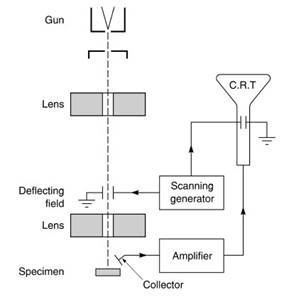
Figure 3. Simplified schematic drawing of a scanning electron microscope (1952)
The collector receives the electrons that are reflected from the specimen surface, and produces an electrical signal that can used to modulate the brightness of the cathode-ray tube used to display the image, as in Knoll’s original electron beam scanner (Figure 2). One of the first (1952) images, of an etched aluminum surface placed at 25 degrees to the beam, shows the three-dimensional effect that is the hallmark of an SEM (Figure 4).

Figure 4. An early visual image (of etched aluminum surface) produced with the first Cambridge SEM; 5-second scan; angle of incidence of 16 kilovolt electrons = 25 degrees; horizontal field width = 37 micrometers
By the early 1960s a succession of Oatley’s students had developed several SEMs that produced high-quality images, although still with substantially lower resolution than TEMs, and consequently were of little interest to the electron microscope community. However, the Cambridge Instrument Company in 1965 marketed an SEM based on Oatley’s work and within a few years had sold several hundred ‘‘Stereoscans’’ (so-named because of the three-dimensional effect); the virtues of the SEM had quickly become apparent to electron microscopists who had actually seen one.
The Stereoscan set the pattern for SEMs marketed by other manufacturers and present instruments are recognizable descendants but with many improvements due to advances in electronics, improved electron-optical components (magnetic lenses, high-intensity field-emission electron guns, etc.), and computer control.
The resolution of an SEM depends not only on the size of the focused electron-scanning spot but also, very importantly, on the scattering of electrons that penetrate the specimen and escape from a larger area of the surface, to be collected by the detector. The depth of penetration of the electrons is a function of their energy and therefore the lowest acceptable energy is used, say 1 kiloelectron volt compared with several 100 kiloelectron volts in a TEM (‘‘acceptable’’ is specified because the diameter of the electron spot increases at low energies due to lens aberrations, and the current in the beam is also reduced).
Advances in electron microscope technology, particularly the field-emission electron gun have enabled very low-energy electrons to be used in an SEM while still achieving good resolution. Typical spot sizes are 1 nanometer with 20 kiloelectron volt energy electrons, 2 nanometers with 1 kiloelectron volt, and 5 nanometers with 200 electron volts.
In an SEM, when the scanning beam hits the specimen not only are secondary electrons with a range of energies emitted but other radiations are as well, in particular x-rays. The energies (or wavelengths) of these depend on the constituents of the specimen surface and if a suitable detector is used, a map of the elements at the surface can be generated, which can be compared with the electron topographical image.
The simplest detector is a cooled silicon diode, doped with lithium, which produces pulses proportional to the energy of the x-ray photons. Better energy resolution can be obtained with a diffracting x-ray spectrometer if one can be accommodated on the SEM near to the specimen. Such microanalyzers were first developed in the 1950s by Raymond Castaing in France and by Ellis Cosslett and Peter Duncumb at the Cavendish Laboratory in Cambridge: these were stand-alone instruments but later this facility was incorporated into many SEMs.
Light is also emitted by cathodoluminescent specimens and can be analyzed in an optical spectrometer; such specimens include biological substances that can be stained with suitable luminescent compounds.
Special types of SEM are used for particular classes of specimen, such as ‘‘wet’’ biological samples that would impair the high vacuum of a conventional SEM with water vapor. The ESEM (environmental SEM), which was first developed by Gerry Danilatos (around 1985) in Australia, operates with a specimen chamber at a relatively high pressure (around 500 pascals, still at low vacuum) so that water does not evaporate from the specimen. The column of the SEM (the region between the electron gun and the specimen) is maintained at high vacuum to enable the electron gun and lenses to operate normally.
Since the introduction of commercial SEMs in 1965, many uses have been found for them, both in advanced research and in routine analysis and imaging for science and industry. Imaging of biological cells, rock specimens, microelectronic components, and metallurgical defects can all be carried out at micrometer and nanometer scale. In fabrication of nanoscale devices and microelectro mechanical systems (MEMS), SEM imaging is an important inspection and metrological technique.
The basic components of electron microscopes continue to be improved; in particular the correction of the aberrations of the electron lenses, and no doubt the SEM will benefit from these developments.
Date added: 2024-03-05; views: 833;