Semiconductors, Postband Theory
The theoretical explanation of transistor action rests upon the concepts of postclassical physics. Important advances took place from the early 1930s onward, when Arnold Sommerfeld, Felix Bloch and co-workers applied quantum theory concepts to the theory of metals. A study of the structure of semiconductor materials applying quantum mechanics was made in Britain by Alan Wilson, 1931-1932. However, only after World War II did clearer pictures begin to emerge which could explain the movement of charge carriers in semiconductor p-n junctions and metal-to-semi- conductor contacts.
Semiconductor research was stimulated during the 1930s by the possibility of military applications in radar detectors and signaling. The major impetus came from the inability of thermionic valves, or vacuum tubes, to operate as fast switches, due to high interelectrode capacitance. This limited their use as signal detectors in radar equipment. Since the point contact diode proved superior in this respect, great efforts were made under wartime conditions to improve their characteristics. Consequently, large well-funded research programs were rapidly instituted by Britain and Germany, and also by the U.S. after 1941.
Although it was known that the addition of minute amounts of certain impurities to bulk semiconductor material altered the characteristics of semiconductor diodes, the effect was difficult to predict. This was because techniques of material purification were not sufficiently developed and therefore inconsistency in batch production was unavoidable. Consequently, work proceeded largely on an ad hoc basis. A method of obtaining a high degree of material purification (zone refining) was described by Petr Kapitza in 1928 but its significance was not realized until much later in the U.S. by William G. Pfann in 1952.
The effects of various doping elements was still not clearly understood in the immediate postwar period. Petritz (U.S.) mentions that even as late as 1948 rectifiers were made with tin-doped germanium in the belief that tin was the doping element, although in fact doping levels were due to impurities within the tin, the tin itself having no electrical effect on the germanium.
Perhaps the most important semiconductor research during World War II was carried out at Purdue University and Bell Laboratories. Purdue concentrated on the study of germanium, Bell on improving silicon point-contact diodes. These devices had already been substantially improved in Britain and elsewhere since the early ‘‘cat’s whisker’’ and now consisted of purified p- or n- doped crystalline material, the metal to semiconductor contact being made by a pointed wire (usually of tungsten or molybdenum) electrically attached by a ‘‘forming’’ process, resulting in a low capacitance rectifying p-n junction. The assembly was then sealed within an inert ambient.
The first p-n junction silicon rectifier was produced by Russell Ohl in 1941 and the presence of group III and V impurities in germanium and silicon was also discovered at about this time (Jack Scaff and William Pfann at Bell Labs). Consequently, it was now possible to make rectifying devices with much higher reverse breakdown voltages and handling much higher powers, as well as multijunction devices such as thyristors. Instead, efforts were concentrated on satisfying wartime requirements and by 1945 Bell (Western Electric) were producing over 50,000 rectifiers monthly.
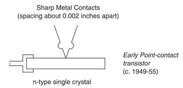
The point-contact transistor (see Figure 7) was invented at Bell laboratories by Walter Brattain and John Bardeen, (1947), following an investigation of the surface properties of semiconductors and an understanding of the role of minority current carriers in electrical conduction. It consisted of two closely spaced wires in electrical contact with a substrate of n-type single-crystal germanium. This device was the product of a two- year goal-oriented research program.

Figure 7. Early point-contact transistor, c. 1949-1955
Realizing its significance, the U.S. government immediately allocated funds for further development. Germanium was chosen because it had been investigated in detail during the war years; it was simpler in structure than compound semiconductors and its melting point (96°C) was lower than silicon (143°C).
Limited production of germanium point contact transistors began in 1951, but the device suffered from considerable defects. Its characteristics varied widely from one device to another, it was electrically unstable, and noise levels were high. Also, device action was extremely complex due to surface effects, making theoretical analysis very difficult. Efforts were therefore concentrated on the more electrically stable junction transistor.
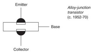
The Czochralski crystal-growing process developed by Jan Czochralski in 1918 was a major advance allowing single crystals to be drawn from the molten state in the form of a p-n-p or n-p-n structure. This method enabled germanium junction transistors to be manufactured in quantity with uniform characteristics. An alternative approach, the germanium alloy-junction transistor (see Figure 8), had the advantage of superior frequency response. The U.S. military realized the significance of these improvements and immediately instituted a ‘‘million a month’’ manufacturing program with Western Electric.

Figure 8. Alloy-junction transistor, c. 1952-1970. The germanium-alloy junction transistor has indium emitter and collector beads alloyed in a germanium base. Parameters are controlled by doping levels, geometry, and surface conditions
The next major step was the successful manufacture of silicon grown-junction transistors by Gordon Teal in 1954. These were single crystal n-p-n junctions grown by the Czochralski process.
Again, this device was of great interest to the military, because it could operate at higher temperatures than germanium and from this time onwards large-scale military involvement took place within the industry, concentrating on silicon technology.
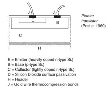
Two significant advances now followed: (1) precise control of junction depth by vapor diffusion; and (2) oxide masking during the diffusion process. Precise control of junction depth resulted in greatly extending high-frequency performance, while oxide masking electrically stabilized the device surface, greatly lowering leakage currents and improving voltage breakdown levels. These developments led to major advances in device construction, most significant by far being the planar transistor (see Figure 9).

Figure 9. Planar transistor, post-1960. Note that the chip is welded to a gold-plated metallic substrate (header). Gold wires are bonded by thermocompression onto the aluminum bonding pads attached to emitter and base. The wires are then connected to electrically isolated posts on the header. The whole assembly is encapsulated in an inert ambient. Device parameters are controlled by geometry and doping levels
This device was so described because the insulating oxide covering the semiconductor surface formed a flat, planar layer. The planar approach offered increased reliability at decreased cost and also permitted large-scale integrated circuit manufacture. Apart from applications such as high-voltage rectifiers and thyristors, it has rendered previous methods of construction obsolete.
In 1960, Bell Laboratories succeeded in growing very thin layers of doped semiconductor crystalline materials upon a silicon semiconductor substrate by vapor deposition. This process is termed epitaxial and it enabled high-resistivity layers to be deposited upon low-resistivity substrates, which cannot be done employing conventional diffusion techniques. It was now possible to construct devices within the epitaxial layer using advantageous doping profiles unattainable by previous means, this greatly assisting the subsequent development of integrated circuitry.
Planar technology is now in almost universal use and enables transistors, capacitors and resistors to be fabricated on a single slice with great precision. Windows are opened in the oxide by selective etching, enabling successive p-n junctions to be formed by impurity diffusion and also allowing metallic interconnections to be deposited. Integrated circuits use these metallic interconnections to link components electrically and achieve the desired circuit configuration.
Since all the devices or integrated circuits on the slice are fabricated simultaneously, variation in their characteristics is minimal and only at the end of the production process are they separated to form ‘‘chips.’’ Electrical connections from the chip to its external packaging are usually made using gold wires, which are attached to the bonding pads by thermocompression bonding. Development of integrated circuitry has largely rested upon silicon, since a stable germanium oxide cannot be grown successfully. However, a number of compound semiconductor materials were increasingly used.
Planar fabrication is particularly suited to the manufacture of metal-oxide field-effect transistors. This led to a whole new development in integrated circuitry from the late 1960s onward. Subsequently, component density per chip has approximately doubled every 18 months (Moore’s law), resulting in great improvements in reliability, speed of operation, reduction in power dissipation and attainment of greater circuit complexity.
Cost per bit has been vastly reduced. For example, a 1-kilobit dynamic random access memory (DRAM) manufactured in 1974 cost one cent per bit. By 1985, a 1-megabit DRAM was being produced as a cost of one thousandth of a cent per bit.
Date added: 2024-03-05; views: 553;
