Semiconductors, Preband Theory
Investigations into the properties of what we now define as semiconductors began in the early nineteenth century. No satisfactory theoretical explanations were possible, and little effort was made to put discoveries to practical use. However, by the beginning of the twentieth century the main distinguishing characteristics of semiconductors (negative temperature coefficient of resistance, asymmetric conduction of electricity in solids, photoelectric effect, photovoltaic effect, large Hall effect, and high thermoelectric power) had been discovered. The one-way conductance, or rectification, property of semiconductors is the characteristic that makes semiconductor devices useful today.
Charles E. Fitts (U.S.) constructed the first practical photocell around 1883-1886 by spreading a semitransparent sheet of gold leaf onto the surface of a selenium layer on a copper backing plate. However, this early work was not pursued for some decades. The main stimulus leading to the development of semiconductor devices came through the need to develop an efficient detector of electromagnetic waves.
Jagadis C. Bose (India) patented the first solid-state point-contact detector in 1904, mentioning a variety of substances including galena (lead sulfide). In 1906 Henry Dunwoody and Greenleaf Whittier Pickard (U.S.) developed detectors using silicon carbide and silicon. In the first decade of the twentieth century many workers were engaged in efforts that led to improvements in detection efficiency for radio receivers (see Radio Receivers, Crystal Detectors and Receivers).
This resulted in production of the so-called ‘‘cat’s whisker,’’ consisting of a rectifying metal to semiconductor contact, the polycrystalline surface of the material being probed by a pointed wire until a rectifying metal-to-semiconductor contact was obtained. The principal substances then being used were silicon and lead sulfide (in the form of galena). By 1909, Karl Baedeker was using the Hall effect to study systematically semiconductor behavior. J. Konigsberger published papers in 1907 and 1914, classifying silicon, selenium, and tellurium as semiconductors (germanium was not added until 1926).
The invention of the thermionic valve and its success as an amplifier soon overshadowed the crystal diode, finally displacing it in radio receivers by about 1926. Consequently, interest waned, although rectification characteristics were still being steadily improved by empirical means. However, a theoretical explanation for the phenomenon of rectification was still lacking. A major factor limiting progress in this respect was that the electrical properties of semiconductor materials are extremely sensitive to the introduction of minute amounts of impurities, and this was not realized at the time.
Since varying amounts of impurities are present within unrefined semiconductor material, device characteristics varied considerably as a consequence. Even if the problem had been appreciated, techniques of crystal purification were not then sufficiently advanced to permit manufacture of material of a suitable quality in order to construct solid-state amplifying devices.
The introduction of the copper or copper oxide rectifier by L.O. Grondahl and P.H. Geiger (Germany) in 1927 was soon followed by the development of efficient selenium rectifiers, which were smaller and lighter for the same operating conditions, and could be operated at higher temperatures. Connected in series and provided with means of cooling, high reverse breakdown voltages were now possible.
Their invention stimulated further interest in semiconductor rectifiers, since they extended existing commercial applications to include rectification in battery chargers and radios. It also raised interest in the possibility of controlling their current by means of a third electrode. Further uses for semiconducting devices followed the introduction of the selenium photovoltaic cell in 1931 by Bruno Lange and colleagues in Germany.
This device operates by generating a voltage across a semiconductor junction when exposed to light, and was soon widely used in photographic exposure meters and applications such as control of artificial lighting, burglar alarms, and the opening and closing of lifts and doors. Photoconductive detectors, whose widespread use also dates from about this time, are devices that vary their conductivity when their surface is exposed to light.
They have the advantage of low cost and quite high sensitivity, although their range of applications is restricted by their relative slowness in operation. A photosensitive material such as cadmium sulfide or cadmium selenide is usually deposited as a polycrystalline film onto a suitable substrate with a honeycomb of electrodes arranged to ensure maximum contact. These cells found an application as photographic exposure meters.
By 1930, little progress had been made in achieving a satisfactory theoretical explanation for the behavior of either semiconductor junctions or metal-to-semiconductor junctions, although a number of rival explanations were now being put forward, including an electrolytic barrier theory, the existence of a Peltier voltage generated by local Joulean heating, and also cold emission across a gap.
Theoretical progress continued to be limited by the lack of reproducibility of experimental results, due to such factors as imperfections in crystal structure, bulk impurities, contact potentials, surface states, photoeffects and heating.
Main techniques used in the investigation of semiconductor material at this time included Hall effect, conductivity, and thermoelectric power measurements. A further factor delaying development was that work in the field of solid-state devices was largely restricted to isolated individuals who lacked the resources necessary to mount a sufficiently large program of investigation.
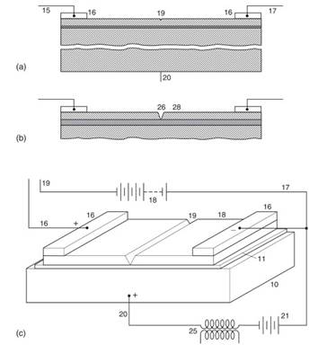
Attempts were made in Germany, Britain, and elsewhere during the interwar years to construct various devices including field-effect transistors (FETs). However, these efforts met with little success. (In field-effect devices a current flows through a semiconductor channel, its width being controlled by means of a gate voltage). Probably the most well-known attempt was that made by Julius Edgar Lilienfield, then professor of physics at Leipzig, who took out patents in 1926 and again in 1928 for a voltage-controlled multilayer structure; one using a thin magnesium layer between semiconducting copper sulfide layers (see Figure 10).

Figure 10. (a) and (b): The construction of a field effect transistor patented by J.E. Lilienfeld in the U.S. in 1933. The construction uses a thin layer of magnesium sandwiched between semiconducting copper sulfide layers. The notch shown in the center of (b) is intended to achieve a narrow cross-section, increasing the electric field at this point and hence the control effect. (c): This device shown with associated circuitry
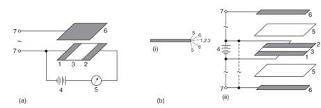
There is no evidence that his devices actually worked. Nor did those of Oskar Heil (Germany) who in 1934 described a field-effect transistor with an insulated gate (see Figure 11). These patents were nevertheless important because their possession conferred priority. Rudolf Hilsch and Robert W. Pohl (Germany), working with alkali halide crystals in 1938, inserted a platinum control grid into the junction space-charge layer of a potassium bromide crystal (the width of which could be calculated), and modulating a signal by applying a grid voltage in similar fashion to that used in thermionic triodes.

Figure 11. (A) and (B): The operation of a field effect transistor patented by O. Heil in Germany in 1934 and Britain in 1935. Heil states therein that ‘‘one or more thin layers of semiconductor traversed by current is or are varied in accordance with control voltage applied to one or more control electrodes arranged to and insulated from said semiconductor layer or layers.’’
(A) illustrates the principle of modulation, the current flowing within the circuit in series with the semiconductor layers being controlled by an alternating voltage applied to a control electrode situated above it. (B) illustrates the circuitry in more detail The unshaded plates shown in the illustration act as insulators
Alkali halides were chosen because large crystals of high purity could be obtained. However, the physical limitations of this approach prevented a useful frequency response being achieved, although their work demonstrated that it was possible to construct a solid-state amplifier. Further efforts to do so were made by William Shockley and Alan Holden (U.S.), working at Bell Laboratories in 1939, but little agreement was found between existing theory and experimental results.
This was due to the lack of appreciation of the effect of minute amounts of unwanted impurities and other crystal imperfections, as well as the importance of the behavior of charge carriers at semiconductor surfaces.
Date added: 2024-03-05; views: 748;
